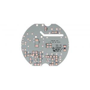
Single Sided PCB GREY SOLDERMASK PCB Printed Circuit Board For Automotive Head Lighting
Details:
1. One of the largest and professional PCB (Printed Circuit Board) manufacturers in China with over 300 staff and 13 years’experience.
2. All kinds of surface finish is accepted,such as ENIG,OSP.Immersion Silver, Immersion Tin, Immersion Gold, Lead-free HASL,HAL.
3. BGA,Blind&Buried Via and Impedance Control is accepted.
4. Advanced production equipment imported from Japan and Germany,such as PCB Lamination Machine, CNC drilling machine,Auto-PTH line,AOI(Automatic Optic Inspection),Probe Flying Machine and so on.
5. Certifications of ISO9001:2008,UL,CE,ROHS,REACH,HALOGEN-FREE is meet.
6. One of the professional SMT/BGA/DIP/PCB Assembly manufacturers in China with 13 years’experience.
7. High speed advanced SMT lines to reach chip +0.1mm on integrated circuit parts.
8. All kinds of integrated circuits is available,such as SO, SOP, SOJ, TSOP, TSSOP, QFP, BGA and U-BGA.
9. Also available for 0201 chip placement, through-hole components insertion and finished products fabrication, testing and package.
10. SMD assembly and through-hole components insertion is accepted.
11. IC preprogramming is also accepted.
12. Available for Function verification and burn in testing.
13. Service for complete unit assembly,for example,plastics, metal box, coil, cable inside .
14. Environmental conformal coating to protect finished PCBA products.
15. Providing Engineering service as end of life components, obsolete component replace and design support for circuit, metal and plastic enclosure.
16. Functional testing,repairs and inspection of the sub-finished and finished goods.
17. High mixed with low volume order is welcomed.
18. Products before delivery should be full quality checked, striving to 100% perfect.
19. One-stop service of PCB and SMT(PCB assembly) is supplied to our customers.
20. Best service with punctual delivery is always provided for our customers.
| PRODUCT’S DETAILS |
| Raw Material | FR-4(Tg 180) |
| Layer Count | 1-Layer |
| Board Thickness | 1.6mm |
| Copper Thickness | 1.0oz |
| Surface Finish | ENIG |
| Solder Mask | Green |
| Silkscreen | White |
| Min. Trace Width/Spacing | 0.075/0.075mm |
| Min. Hole Size | 0.3mm |
| Hole Wall Copper Thickness | ≥20μm |
| Measurement | 30×10mm |
| Packaging | Inner: Vacuum-packed in soft plastic bales
Outer: Cardboard Cartons with double straps |
| Application | Communication,automobile,cell,computer,medical |
| Advantage | Competitive Price,Fast Delivery,OEM&ODM,Free Samples, |
| Special Requirements | Buried And Blind Via, Impedance Control, Via Plug,
BGA Soldering And Gold Finger Are Acceptable |
| Certification | UL,ISO9001:2008,ROHS,REACH,SGS,HALOGEN-FREE |
| PRODUCTION CAPABILITY OF PCB |
PROCESS Engineer | ITEMS Item |
PRODUCTION CAPABILITY Manufacturing Capability |
| Laminate | Type | FR-1,FR-5,FR-4 High-Tg,ROGERS,ISOLA,ITEQ,
ALUMINUM,CEM-1,CEM-3,TACONIC,ARLON,TEFLON |
| Thickness | 0.2~3.2mm |
| Production Type | Layer Count | 2L-16L |
| Surface Treatment | HAL,Gold Plating,Immersion Gold,OSP,
Immersion Silver,Immersion Tin,Lead Free HAL |
| Cut Lamination | Max. Working Panel size | 1000×1200mm |
| Inner Layer | Internal Core Thickness | 0.1~2.0mm |
| Internal width/spacing | Min: 4/4mil |
| Internal Copper Thickness | 1.0~3.0oz |
| Dimension | Board Thickness Tolerance | ±10% |
| Interlayer Alignment | ±3mil |
| Drilling | Manufacture Panel Size | Max: 650×560mm |
| Drilling Diameter | ≧0.25mm |
| Hole Diameter Tolerance | ±0.05mm |
| Hole Position Tolerance | ±0.076mm |
| Min.Annular Ring | 0.05mm |
| PTH+Panel Plating | Hole Wall copper Thickness | ≧20um |
| Uniformity | ≧90% |
| Outer Layer | Track Width | Min: 0.08mm |
| Track Spacing | Min: 0.08mm |
| Pattern Plating | Finished Copper Thickness | 1oz~3oz |
| EING/Flash Gold | Nickel Thickness | 2.5um~5.0um |
| Gold Thickness | 0.03~0.05um |
| Solder Mask | Thickness | 15~35um |
| Solder Mask Bridge | 3mil |
| Legend | Line width/Line spacing | 6/6mil |
| Gold Finger | Nickel Thickness | ≧120u〞 |
| Gold Thickness | 1~50u〞 |
| Hot Air Level | Tin Thickness | 100~300u〞 |
| Routing | Tolerance of Dimension | ±0.1mm |
| Slot Size | Min:0.4mm |
| Cutter Diameter | 0.8~2.4mm |
| Punching | Outline Tolerance | ±0.1mm |
| Slot Size | Min:0.5mm |
| V-CUT | V-CUT Dimension | Min:60mm |
| Angle | 15°30°45° |
| Remain Thickness Tolerance | ±0.1mm |
| Beveling | Beveling Dimension | 30~300mm |
| Test | Testing Voltage | 250V |
| Max.Dimension | 540×400mm |
| Impedance Control |
Tolerance | ±10% |
| Aspect Ration | 12:1 |
| Laser Drilling Size | 4mil(0.1mm) |
| Special Requirements | Buried And Blind Via, Impedance Control, Via Plug,
BGA Soldering and Gold Finger Are Acceptable |
| OEM&ODM Service | Yes |
What We Can Do for You?
With over 13 years experience, we offer OEM & ODM PCB Layout, PCB Design, PCB manufacturing and PCB Assembly in single-sided PCB Board, double-sided PCB and Multilayer Printed Circuit Board service to our customers, with total production capacity of 300,000 sqm/month.
How to get quick quotation?

| Step 1 Please send us Gerber file with these format: .CAD / .Gerber / .PCB / .DXP / .P-CAD, etc |
| Step 2 Also please provide us the below details for quick quotation: |
| Board material: Fr - 4 / CEM - 1 / CEM - 3 / 22F / Fr - 1 / others |
| Material brand: SY / KB / Rogers (optional) |
| Material Specification:High Tg / copper based / aluminum based or others (optional) |
| Board thickness: 0.1 - 6.0 mm |
| Copper thickness: 0.05 Oz - 8 Oz ( 17 um - 288 um ) |
| Surface Treatment: OSP / ENIG / HASL / Lead Free HASL / Immersion Tin / Immersion Sin |
| Color of solder mask and silk print: Green / red / blue / black / white / yellow ,etc |
| Board size and quantity |
| If you don't have Gerber file, please provide us the imfomation as step 2 or post your PCB Board to us for clone. |
| SAMPLE: |
| Board Basic Info - SAMPLE | | Board material | Fr - 4 | | Material brand | KB | | Material Specification | Tg 170 | | Board thickness | 1.6 mm | | Copper thickness | 1 Oz | | Surface Treatment | ENIG | | Solder mask / Silk print | Green / White | | Board size | 100 mm * 100 mm | | Quantity | 10k | |
Lead Time
| Layer count | Sample lead time/workday | Batch lead time/workday |
| 1-2L | 2 | 6 |
| 4L | 5 | 8 |
| 6L | 5 | 9 |
| 8L | 6 | 10 |
| 10L | 8 | 10 |
| 12L | 8 | 12 |
| 14L | 10 | 15 |
| 16L | 10 | 18 |
| 18-40L (Up to difficulty) | at least 18 | at least 24 |
| P.S. For HDI, Blind/Buried Hole PCB: Regular Lead Time + 3 workdays |
Q1: I am used to designing in metric units while the website is specified in imperial units.
A: When requesting an online quote, the quote form can handle mm units as well as inches for dimensions.
Q2: How do I specify internal cutouts/milling in my design?
A: All internal cutouts/slots/milling should be specified on the same layer is the board outline. The the minimum routable slot size is 32 mils. During order time, please state this requirement in the "Special Request" section so that our CAM engineers is aware of it. This is not something we encounter
Q3: What are the available holes sizes?
A: 14 mils to 150 mils - 1 mil increments 150 mils to 200 mils - 5 mil increments above 200 mils - holes would be routed out We only use drills in imperial units. Files submitted in metric units (mm) would be converted to imperial units (mils) and rounded up to the next mil.
Now send us your inquiry, and you will be replied within 8 hours!
Little knowledge - Consideration about PCB fabrication
When placed an order of PCBs (printed circuit boards), you should spend time to considerate the basic factors including PCB board substrate material, layer count, board size, board thickness, copper thickness, surface finish, solder mask, silkscreen, blind vias, buried vias, through-hole plating, SMT and so on. When all the factors are checked and confirmed with the engineers, we highly recommended sample tested before the real fabrication of your PCB boards. If all things go well, fabrication could be started right away. However, it may need to do some modification if customer is not satisfied with the sample.