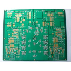
4Layer Entertainment Systems Audio Amplifier PCB , Quick Turn PCB Fabrication
Brief Description:
For 94V0 double sided high frequency PCB Board manufacturing, FOISON meets UL and RoHS compliant. The layer count of this green solder high frequency PCB Board is 4, with 1.6 mm board thickness. And the minimum Line width and space of the PCB are 0.1 and 0.11 mm.
Quick Details
- One of the largest PCB(Printed Circuit Board) manufacturers in China with over 300 staff.
- BGA,Blind&Buried Vias and Impedence Control is accepted.
- One of the professional PCB manufacturers in China with 13 years’ experience.
- Certifications of ISO9001:2008,UL,CE,ROHS,REACH,HALOGEN-FREE is meet.
- One-stop service of PCB with assembly is supplied to our customers.
- Best service with quick response is always provided for our customers.
- All kinds of surface finish is accepted,such as ENIG,OSP.Immersion Silver,Immersion Tin, Immersion Gold, Lead-free HASL,HAL.
- Advanced production equipment imported from Japan and Germany,such as PCB Lamination Machine, CNC drilling machine,Auto-PTH line, AOI(Automatic Optic Inspection),Probe Flying Machine and so on.
- Good quality with competitive price for all kinds of PCB manufactured by FOISON PCB.
Characteristics:
1. Professional PCB manufacturer.
2. PCBA,OEM,ODM service are provided.
3. Gerber file needed.
4. Products are 100% E-tested.
5. Quality guarantee and professional after-sale service
| PRODUCTION CAPABILITY OF PCB |
PROCESS Engineer | ITEMS Item |
PRODUCTION CAPABILITY Manufacturing Capability |
| Laminate | Type | FR-1,FR-5,FR-4 High-Tg,ROGERS,ISOLA,ITEQ,
ALUMINUM,CEM-1,CEM-3,TACONIC,ARLON,TEFLON |
| Thickness | 0.2~3.2mm |
| Production Type | Layer Count | 2L-16L |
| Surface Treatment | HAL,Gold Plating,Immersion Gold,OSP,
Immersion Silver,Immersion Tin,Lead Free HAL |
| Cut Lamination | Max. Working Panel size | 1000×1200mm |
| Inner Layer | Internal Core Thickness | 0.1~2.0mm |
| Internal width/spacing | Min: 4/4mil |
| Internal Copper Thickness | 1.0~3.0oz |
| Dimension | Board Thickness Tolerance | ±10% |
| Interlayer Alignment | ±3mil |
| Drilling | Manufacture Panel Size | Max: 650×560mm |
| Drilling Diameter | ≧0.25mm |
| Hole Diameter Tolerance | ±0.05mm |
| Hole Position Tolerance | ±0.076mm |
| Min.Annular Ring | 0.05mm |
| PTH+Panel Plating | Hole Wall copper Thickness | ≧20um |
| Uniformity | ≧90% |
| Outer Layer | Track Width | Min: 0.08mm |
| Track Spacing | Min: 0.08mm |
| Pattern Plating | Finished Copper Thickness | 1oz~3oz |
| EING/Flash Gold | Nickel Thickness | 2.5um~5.0um |
| Gold Thickness | 0.03~0.05um |
| Solder Mask | Thickness | 15~35um |
| Solder Mask Bridge | 3mil |
| Legend | Line width/Line spacing | 6/6mil |
| Gold Finger | Nickel Thickness | ≧120u〞 |
| Gold Thickness | 1~50u〞 |
| Hot Air Level | Tin Thickness | 100~300u〞 |
| Routing | Tolerance of Dimension | ±0.1mm |
| Slot Size | Min:0.4mm |
| Cutter Diameter | 0.8~2.4mm |
| Punching | Outline Tolerance | ±0.1mm |
| Slot Size | Min:0.5mm |
| V-CUT | V-CUT Dimension | Min:60mm |
| Angle | 15°30°45° |
| Remain Thickness Tolerance | ±0.1mm |
| Beveling | Beveling Dimension | 30~300mm |
| Test | Testing Voltage | 250V |
| Max.Dimension | 540×400mm |
| Impedance Control |
Tolerance | ±10% |
| Aspect Ration | 12:1 |
| Laser Drilling Size | 4mil(0.1mm) |
| Special Requirements | Buried And Blind Via, Impedance Control, Via Plug,
BGA Soldering and Gold Finger Are Acceptable |
| OEM&ODM Service | Yes |
What We Can Do for You?
With over 13 years experience, we offer OEM & ODM PCB Layout, PCB Design, PCB manufacturing and PCB Assembly in single-sided PCB Board, double-sided PCB and Multilayer Printed Circuit Board service to our customers, with total production capacity of 300,000 sqm/month.
How to get quick quotation?

| Step 1 Please send us Gerber file with these format: .CAD / .Gerber / .PCB / .DXP / .P-CAD, etc |
| Step 2 Also please provide us the below details for quick quotation: |
| Board material: Fr - 4 / CEM - 1 / CEM - 3 / 22F / Fr - 1 / others |
| Material brand: SY / KB / Rogers (optional) |
| Material Specification:High Tg / copper based / aluminum based or others (optional) |
| Board thickness: 0.1 - 6.0 mm |
| Copper thickness: 0.05 Oz - 8 Oz ( 17 um - 288 um ) |
| Surface Treatment: OSP / ENIG / HASL / Lead Free HASL / Immersion Tin / Immersion Sin |
| Color of solder mask and silk print: Green / red / blue / black / white / yellow ,etc |
| Board size and quantity |
| If you don't have Gerber file, please provide us the imfomation as step 2 or post your PCB Board to us for clone. |
| SAMPLE: |
| Board Basic Info - SAMPLE | | Board material | Fr - 4 | | Material brand | KB | | Material Specification | Tg 170 | | Board thickness | 1.6 mm | | Copper thickness | 1 Oz | | Surface Treatment | ENIG | | Solder mask / Silk print | Green / White | | Board size | 100 mm * 100 mm | | Quantity | 10k | |
Lead Time
| Layer count | Sample lead time/workday | Batch lead time/workday |
| 1-2L | 2 | 6 |
| 4L | 5 | 8 |
| 6L | 5 | 9 |
| 8L | 6 | 10 |
| 10L | 8 | 10 |
| 12L | 8 | 12 |
| 14L | 10 | 15 |
| 16L | 10 | 18 |
| 18-40L (Up to difficulty) | at least 18 | at least 24 |
| P.S. For HDI, Blind/Buried Hole PCB: Regular Lead Time + 3 workdays |
Q1: I am used to designing in metric units while the website is specified in imperial units.
A: When requesting an online quote, the quote form can handle mm units as well as inches for dimensions.
Q2: How do I specify internal cutouts/milling in my design?
A: All internal cutouts/slots/milling should be specified on the same layer is the board outline. The the minimum routable slot size is 32 mils. During order time, please state this requirement in the "Special Request" section so that our CAM engineers is aware of it. This is not something we encounter.
Q3: What are the available holes sizes?
A: 14 mils to 150 mils - 1 mil increments 150 mils to 200 mils - 5 mil increments above 200 mils - holes would be routed out We only use drills in imperial units. Files submitted in metric units (mm) would be converted to imperial units (mils) and rounded up to the next mil.
Now send us your inquiry, and you will be replied within 8 hours!
Little knowledge - High Tg PCB
The glass transition temperature (Tg) is an important normative dimension for the base material that determines the temperature at which the resin matrix converts from a glassy, brittle condition into a soft, elastic one.
Normally high Tg refers to high heat resistance in PCB raw material.
The standard Tg for copper clad laminate is between 130 – 140℃. High Tg is generally greater than 170℃, and middle Tg is generally greater than 150℃. Basically the printed circuit board with Tg≥170℃, we call high Tg PCB.
The higher of TG value, the better of pcb high temperature resistance.